Printed Circuit Board Basics: From Design to Final Artwork
Printed Circuit Boards (PCBs) are the backbone of modern electronics, forming the foundation on which all electronic components are assembled and connected. From consumer electronics and industrial equipment to automotive systems and medical devices, PCBs ensure reliable electrical performance and compact system design. Understanding the journey of a printed circuit board from design to final artwork is essential for engineers, manufacturers, and businesses seeking high-quality PCB fabrication and assembly solutions.
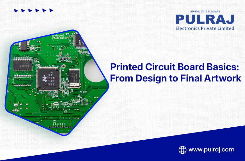
At Pulraj, a leading Printed Circuit Board Basics Manufacturer in India we specialize in precision-driven PCB design support, fabrication, and assembly services that ensure performance, reliability, and scalability.
What Is a Printed Circuit Board (PCB)?
A Printed Circuit Board is a flat board made from insulating material, typically FR-4, with conductive copper tracks etched onto its surface. These copper traces create electrical pathways that connect components such as resistors, capacitors, integrated circuits, and connectors.
PCBs replace traditional point-to-point wiring, offering better reliability, reduced size, and improved electrical performance. Depending on application needs, PCBs can be single-layer, double-layer, or multilayer designs.
Step 1: PCB Design and Concept Development
The PCB development process begins with understanding the functional requirements of the electronic circuit. Designers analyze factors such as voltage levels, current flow, signal speed, thermal performance, and environmental conditions.
Using advanced PCB design software, engineers convert schematic diagrams into a digital layout. Key considerations at this stage include:
- Component placement for optimal signal flow
- Trace width and spacing
- Power and ground plane design
- EMI/EMC control
- Design for Manufacturability (DFM)
A well-optimized PCB design reduces production errors, enhances performance, and ensures long-term reliability.
Step 2: Schematic Capture and Netlist Creation
Once the circuit logic is finalized, engineers create a schematic diagram, which represents all components and their electrical connections. From this schematic, a netlist is generated.
The netlist acts as a roadmap, defining how every component pin connects across the PCB. Accuracy at this stage is critical, as errors can lead to short circuits, open connections, or functional failures in the final board.
Pulraj emphasizes rigorous verification at the schematic stage to minimize design revisions later in the process.
Step 3: PCB Layout and Routing
The PCB layout stage transforms the schematic into a physical board design. Components are placed on the board, and copper traces are routed to establish electrical connections.
Key layout considerations include:
- Signal integrity and impedance control
- High-speed and high-frequency routing rules
- Thermal management for heat-generating components
- Clearance and creepage distances
- Layer stack-up for multilayer PCBs
Proper routing ensures stable electrical performance and prevents issues such as signal loss, crosstalk, and overheating.
Step 4: Design Rule Check (DRC) and Verification
Before moving to manufacturing, the PCB design undergoes Design Rule Checks (DRC) and Electrical Rule Checks (ERC). These automated checks ensure compliance with fabrication and assembly standards.
Verification includes:
- Trace width and spacing validation
- Via size and pad alignment checks
- Component footprint accuracy
- Electrical connectivity confirmation
This step helps identify errors early, saving time and reducing production costs.
Step 5: Generating PCB Final Artwork
The final artwork is one of the most crucial deliverables in the PCB manufacturing process. It consists of Gerber files, drill files, and fabrication drawings that define every layer of the PCB.
PCB artwork includes:
- Copper layers (top and bottom)
- Solder mask layers
- Silkscreen layers
- Drill and routing data
- Assembly drawings
These files serve as precise instructions for PCB fabrication machines. High-quality PCB artwork ensures accurate etching, drilling, and component placement during production.
At Pulraj, every artwork file is thoroughly reviewed to ensure compatibility with manufacturing tolerances.
Step 6: PCB Fabrication Process
Once the artwork is approved, the PCB moves into fabrication. The process typically includes:
- Copper lamination on the base substrate
- Photoresist application and UV exposure using artwork films
- Etching to remove unwanted copper
- Drilling for vias and component holes
- Plating for electrical conductivity
- Solder mask application
- Silkscreen printing for component identification
Each step requires strict quality control to ensure the PCB meets performance and durability standards.
Step 7: PCB Assembly and Final Inspection
After fabrication, the board undergoes PCB assembly, where components are mounted using Surface Mount Technology (SMT) or Through-Hole Technology (THT).
Assembly is followed by inspection and testing, including:
- Automated Optical Inspection (AOI)
- In-circuit testing (ICT)
- Functional testing
These inspections confirm that the PCB operates as intended before final delivery.
Importance of Professional PCB Design and Artwork
A well-designed PCB with accurate final artwork offers multiple benefits:
- Improved electrical performance
- Reduced manufacturing defects
- Faster time-to-market
- Lower rework and maintenance costs
- Enhanced product reliability
Partnering with an experienced PCB solutions provider like Pulraj ensures that every stage—from design to final artwork and assembly—is handled with precision and industry best practices.
Why Choose Pulraj for PCB Solutions?
Pulraj delivers end-to-end printed circuit board design, fabrication, and assembly services tailored to diverse industry needs. Our expertise ensures seamless transitions from concept to final product while maintaining strict quality standards.
Key advantages of working with Pulraj include:
- Advanced PCB design and layout support
- Accurate Gerber and final artwork generation
- High-quality PCB fabrication and assembly
- Strict quality inspection and testing
- Scalable solutions for prototypes and mass production
Understanding **printed circuit board basics—from design to final artwork—**is essential for developing reliable and efficient electronic products. Each step plays a critical role in ensuring functionality, durability, and manufacturability.
At Pulraj, a Top Printed Circuit Board Basics Supplier in Mumbai expertise in PCB design, artwork generation, fabrication, and assembly, businesses can confidently bring innovative electronic products to market with superior quality and performance.